Optimization of power density through GaN semiconductors

For some time now, silicon-based power transistors (MOSFETs) have been considered the gold standard in the low to medium power segment of power supply solutions. They have maintained their position as a standard component in converter technology to this day thanks to the continued development of the technology over the decades and their large-scale production.
The further development of III-V semiconductors has allowed for the evolution of power transistors based on gallium nitride (GaN), which offer significant advantages due to a band gap that is three times larger than that of silicon.
One key advantage is the material’s breakdown field strength – higher by a factor of 10 – which allows for the construction of thinner structures with the same reverse voltage. This makes it possible to significantly reduce the on-state resistance RDS,on of the transistor, resulting in lower conduction losses. Increased electron mobility compared to silicon transistors also leads to lower switching losses and enables higher switching velocities.
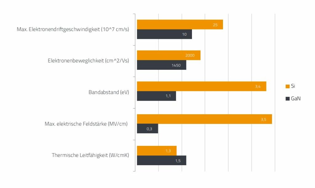
Comparison of selected semiconductor properties
Small and powerful
A common objective when designing power supply solutions such as power packs and charging units is the maximization of efficiency and power density. Two limiting design elements are always the maximum dissipated power in the form of heat loss through the housing and the spatial requirements of the electronic components themselves.
This is precisely where the advantages of the aforementioned GaN semiconductors come in. The lower switching and conduction losses equal less heat dissipation, which, in terms of device design, results in smaller packaging surface necessary for heat dissipation. In addition, higher switching frequencies of the electronic converters allow for the usage of smaller magnetic components such as coils and converters. As a result, GaN technology enables increased power density and optimization of the device’s weight while retaining the same performance levels seen in the classic silicon transistor solutions thanks to the smaller size.

Wafer-inspection during quality assurance
Why GaN is the future of charging
The demand for maximum efficiency and power density results from normative requirements as much as it does from space limitations or purely practical and aesthetic reasons. Everyday examples include the lightest and smallest laptop or phone chargers reducing luggage weight when traveling, or e-bike chargers no longer being an issue when undertaking a longer trip.
Seen from an ecological perspective, GaN semiconductors also help reduce the user’s CO2 footprint thanks to a clear reduction in energy losses for the same amount of charging. GaN semiconductor-based power packs and chargers are not that widespread today. However, recent studies have stated that they will be present in more than 50% of all newly manufactured devices by 2025.
We would be more than happy to advise you on the ideal specification for your product. During the subsequent product development phase, our experienced engineers will ensure that you receive a product that is both state-of-the-art and tailored to your exact needs.
For more information about FRIWO and our products & services, click here.